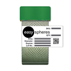

EasySpheres is the exclusive worldwide provider of high quality, first run Solder Balls at reasonable quantities and excellent prices. We endeavor to become your first source and technical guide to many of the solder attach and bumping challenges that you face today.
We maintain a large inventory of sphere alloys and sizes, and specialize in the fulfillment of small orders. We are always able to guarantee quick delivery. This is accomplished in the specialized manner in which we manage our inventory, shipping all orders within 24 hours, and making your ordering process as easy and efficient as possible.
Read More
The move to lead free (Pb-free) electronics by the commercial industry has resulted in an increasing
Read More »
6 Common Mistakes of BGA ReworkBall Grid Array rework is one of the most challenging procedures pe
Read More »EasySpheres has the satisfaction of working with many of the innovators in the US and Worldwide Electronics Manufacturing Community. Serving the Aerospace, Consumer, EMS, Medical, Semiconductor, BGA Rework manufacturing markets now for over 12 years. Some of our customers include:


EasySpheres is the exclusive worldwide provider of high quality, first run Solder Balls at reasonable quantities and excellent prices. We endeavor to become your first source and technical guide to many of the solder attach and bumping challenges that you face today.
We maintain a large inventory of sphere alloys and sizes, and specialize in the fulfillment of small orders. We are always able to guarantee quick delivery. This is accomplished in the specialized manner in which we manage our inventory, shipping all orders within 24 hours, and making your ordering process as easy and efficient as possible.
The concept of EasySpheres was born out of the idea that many end user applications for solder balls require smaller unit quantities than most sphere manufacturers are willing to provide. Combine this concept with guaranteed immediate delivery, easy internet ordering and fulfillment, and a broad range of stock on most popular alloys and sizes, and you have....EasySpheres!
EasySpheres is a leading global supplier of high performance interconnect materials and related services for the electronic and micro-component assembly markets.
Please set up EasySpheres as your preferred vendor today. The PDF link prodvided below should give you all the information you require:

(Ball Grid Array) A popular surface mount chip package that uses a grid of solder balls as its connectors.
Available in plastic and ceramic varieties, BGA is noted for its compact size, high lead count and low inductance, which allows lower voltages to be used. BGA chips are easier to align to the printed circuit board, because the leads, which are called "solder balls" or "solder bumps," are farther apart than leaded packages.
Since the leads are underneath the chip, BGA has led the way to chip scale packaging (CSP) where the package is not more than 1.2x the size of the semiconductor die itself. See surface mount, chip package, MicroBGA and flip chip.


These are the undersides of BGA packages showing the solder balls. The small one on the ruler is a µBGA (MicroBGA) chip from Tessera. Using the entire square of the chip package for leads is an advantage of the BGA method. (Image samples courtesy of Amkor Technology, Inc.).
The BGA is descended from the pin grid array (PGA), which is a package with one face covered (or partly covered) with pins in a grid pattern which, in operation, conduct electrical signals between the integrated circuit and the printed circuit board (PCB) on which it is placed. In a BGA the pins are replaced by pads on the bottom of the package, each initially with a tiny solder ball stuck to it. These solder spheres can be placed manually or by automated equipment, and are held in place with a tacky flux.[1] The device is placed on a PCB with copper pads in a pattern that matches the solder balls. The assembly is then heated, either in a reflow oven or by an infrared heater, melting the balls. Surface tension causes the molten solder to hold the package in alignment with the circuit board, at the correct separation distance, while the solder cools and solidifies, forming soldered connections between the device and the PCB.
In more advanced technologies, solder balls may be used on both the PCB and the package. Also, in stacked multi-chip modules, solder balls are used to connect two packages.
High density
The BGA is a solution to the problem of producing a miniature package for an integrated circuit with many hundreds of pins. Pin grid arrays and dual-in-line surface mount (SOIC) packages were being produced with more and more pins, and with decreasing spacing between the pins, but this was causing difficulties for the soldering process. As package pins got closer together, the danger of accidentally bridging adjacent pins with solder grew. BGAs do not have this problem if the solder is factory-applied to the package.
Heat conduction
A further advantage of BGA packages over packages with discrete leads (i.e. packages with legs) is the lower thermal resistance between the package and the PCB. This allows heat generated by the integrated circuit inside the package to flow more easily to the PCB, preventing the chip from overheating.
Low-inductance leads
The shorter an electrical conductor, the lower its unwanted inductance, a property which causes unwanted distortion of signals in high-speed electronic circuits. BGAs, with their very short distance between the package and the PCB, have low lead inductances, giving them superior electrical performance to pinned devices.